logo
Products
Home / Products / Waffle Pack Chip Trays /

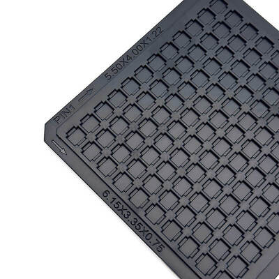
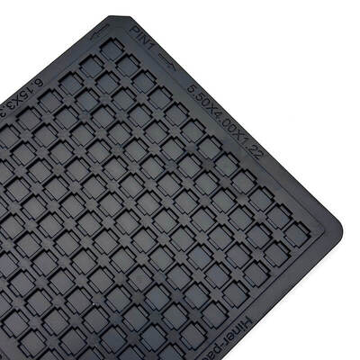
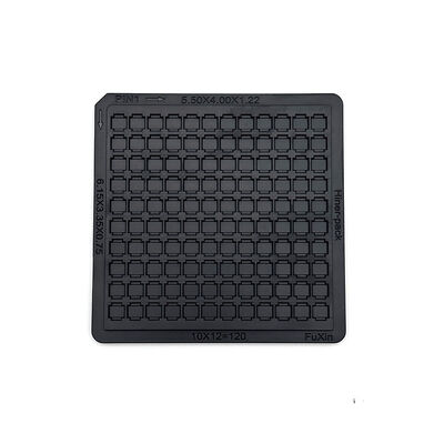
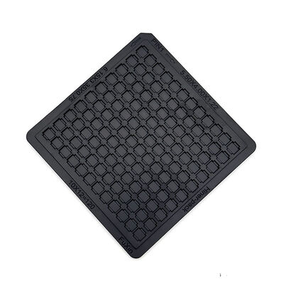
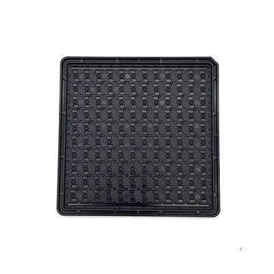
Waffle Pack Chip Trays for Protecting Semiconductor IC Chips from Friction and Mechanical Damage

Waffle Pack Chip Trays for Protecting Semiconductor IC Chips from Friction and Mechanical Damage

Brand Name: Hiner-pack
Model Number: HN25204
MOQ: 1000
Price: $1.35~$2.68(Prices Are Determined According To Different Incoterms And Quantities)
Payment Terms: T/T
Supply Ability: 2000PCS/Day
Detail Information
Place of Origin:
China
Certification:
ROHS, ISO
Tray Weight:
Varies, Typically Up To 500 Grams Per Cavity
Color:
Black
Quality Assurance:
Delivery Guarantee, Reliable Quality
Outline Line Size:
101.6×101.6×5.5 Mm
Cavity Size:
5.25×4.0×1.2 Mm
Incoterms:
EXW, FOB, CIF, DDU, DDP
Mold Type:
Injection
Reusable:
Yes
Tray Shape:
Rectangular
Clean Class:
General And Ultrasonic Cleaning
Ic Type:
BGA,QFP,QFN,LGA,PGA
Packing Level:
Transport Package
Warpage:
Warpage MAX 0.23mm
Capacity:
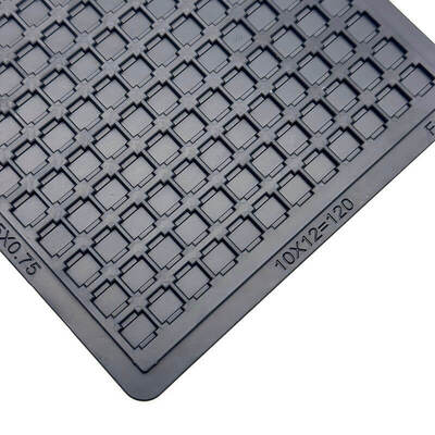
12×14=168 PCS
Packaging Details:
CARTON, PALLET
Supply Ability:
2000PCS/Day
Product Description
Waffle Pack Chip Trays for Protecting Semiconductor IC Chips from Friction and Mechanical Damage
Precise matrix cavities separate delicate IC chips and limit abrasion during handling. Stable anti-static performance stops electrostatic harm to sensitive semiconductor parts. Want dependable protection for high-value components through repeated stacking cycles? Consistent shielding cuts part damage risk.


Fit ESD controlled workshops and automated test equipment. Handle chip sorting, electrical inspection and cross plant transfer. Keep components safe from packing until final assembly. Gain reliable performance favored by IC packaging and semiconductor manufacturers.


Full custom service available. Tune cavity shape, arrangement and outer dimensions to fit special chip outlines and automation needs. Customized structures simplify production flows and lower component loss for mass production orders.

Key Features/ Benefits 
  • Stable conductive ESD performance
  • Precision matrix cavity layout
  • Resist friction and mechanical scratches
  • Secure chip holding
  • Support custom specifications
  • The factory has ISO certification, and the products comply with the RoHS standard.
Specifications
Brand Hiner-pack
Model HN25204
Color Black
Resistance 1.0×10⁴ - 1.0×10¹¹ Ω
Outline Line Size 101.6×101.6×5.5 mm
Cavity Size 5.25×4.0×1.2 mm
Matrix QTY 12×14=168 PCS
Warpage MAX 0.23mm
Service Accept OEM, ODM
Custom Pocket Options Available
Applications
Serve semiconductor IC testing, component sorting and precision inspection. Match automatic handling machines inside ESD production zones.

Fit temporary chip storage, internal transit and component packaging. Widely used by IC packaging factories and electronic manufacturers.
Customized Services
Customization service stands as core support for diverse semiconductor projects. Pocket dimensions, cavity layout, marking positions and outer sizes can all be developed as requested. Professional technical team backs prototype evaluation, sample testing and mass production. Flexible adjustments meet unique automation and packaging needs to cut component waste for different chip types.
About Us:
Hiner-pack® was founded in 2013. It is a high-tech enterprise that integrates Design, R&D, Manufacturing, Sales of IC packaging and testing, as well as semiconductive wafer fabrication process in automated handling, carrying, and transportation to provide customers with turnkey services.

Why Choose Us:

  • Rich experience in JEDEC / IC / Waffle pack trays
  • In-house mold design capability
  • Fast prototype development
  • Strict QC process
  • Stable supply for global semiconductor customers